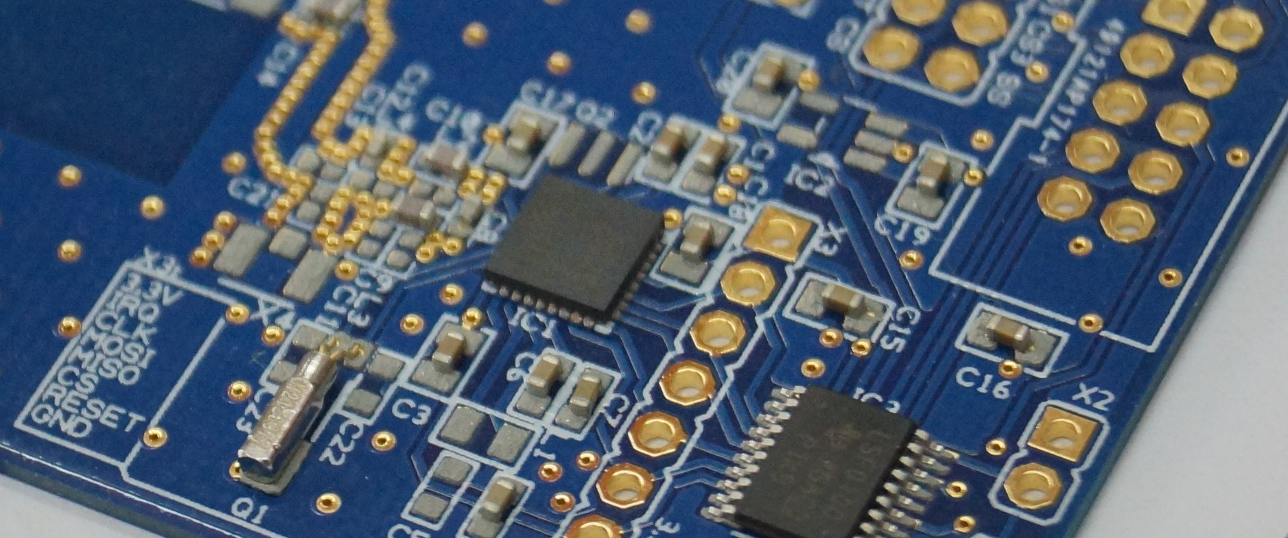
 Pcb
Pcb
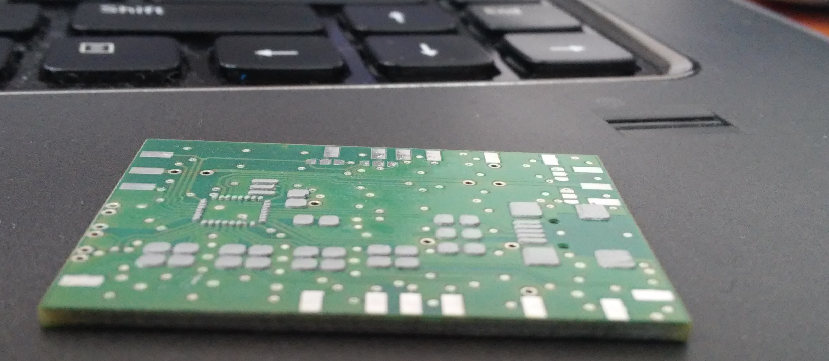
 Assembly
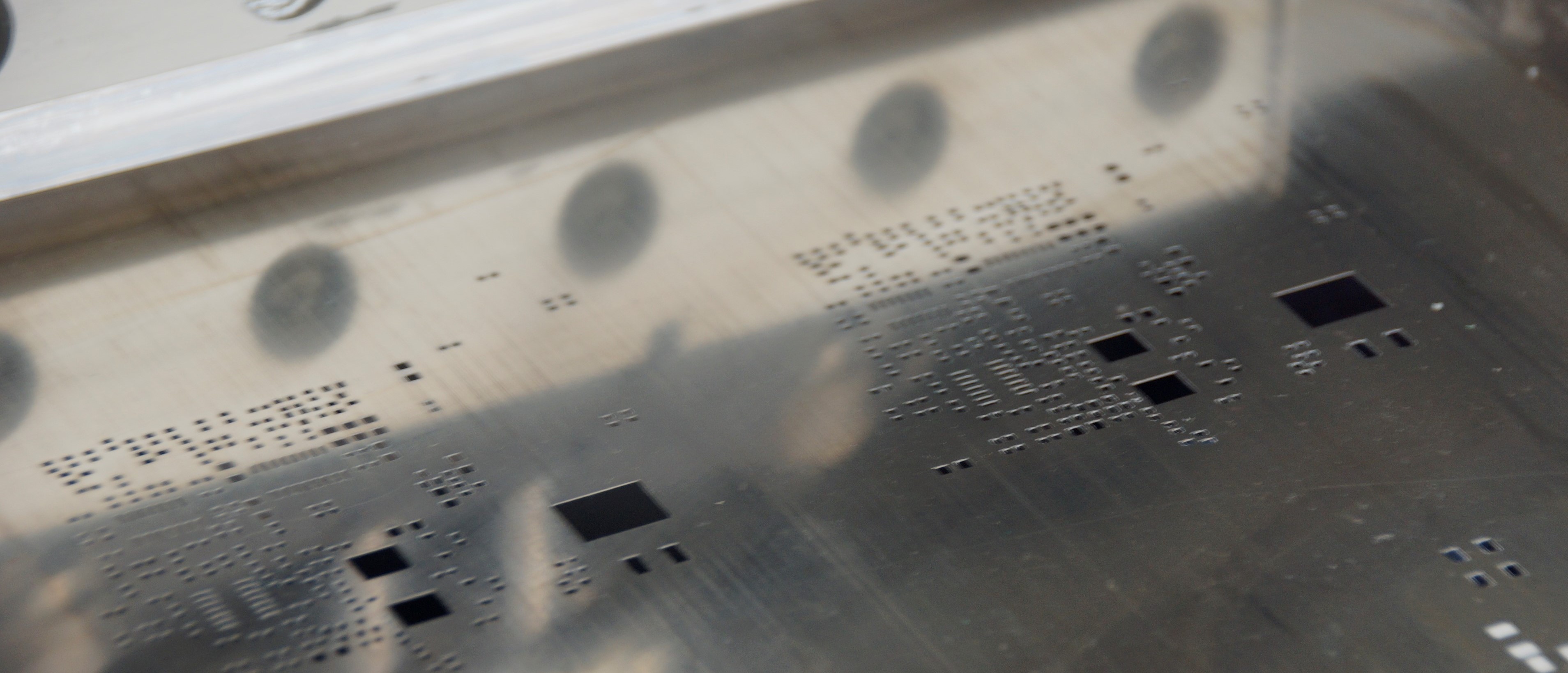
 Stencil
 Cable
Cable
 Test
Test
 Design
Solder Paste Stencil
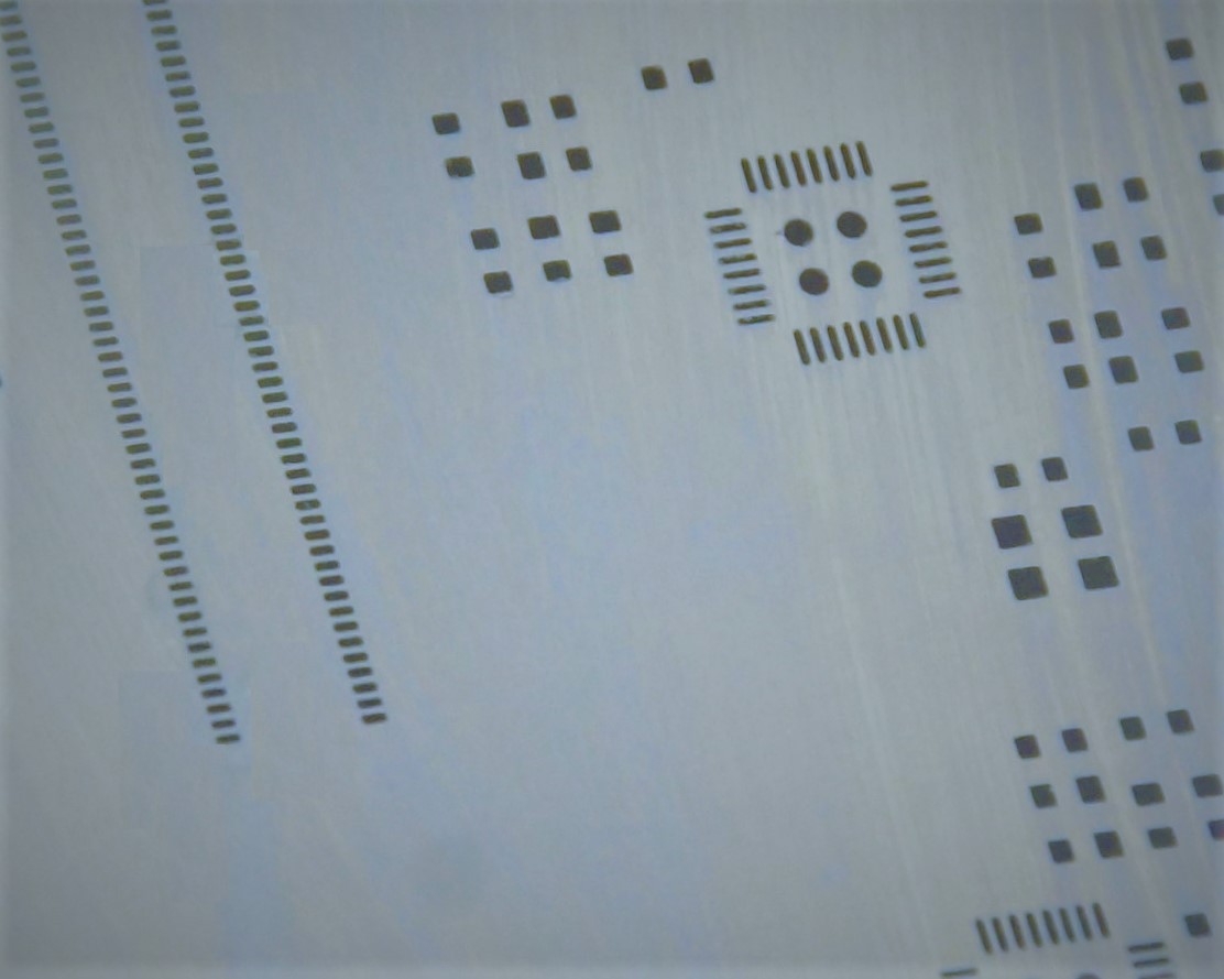
Solder Paste Stencils
Solder paste stencils are a critical tool in the PCB assembly process.
They are used to apply solder paste precisely to component pads before reflow soldering.
The quality and precision of the stencil directly affect the reliability and appearance of the final assembly.
We offer a wide range of stencil types, including laser-cut and chemically etched stencils.
Laser-cut stencils are the preferred choice for medium to large production runs due to their superior precision and durability.
Etched stencils, on the other hand, are more economical and are often used for prototypes and low-volume production.
Our stencils are produced from high-quality nickel silver or stainless steel, depending on your application.
While etched nickel silver stencils offer a cost-effective solution for sampling and early-stage designs,
laser-cut stencils provide better paste definition and are more consistent over time — making them ideal for repeatable and scalable production.
LASER CUT PROCESS
| Lead Time: | 1–3 Days |
|---|---|
| Material: | Nickel Silver |
| Max Size: | 600 × 800 mm |
| Thickness: | 100 μm, 120 μm, 150 μm |
| Smallest Aperture Size: | 2 mils / 0.05 mm |
| Pads: | Unlimited |
| Text Characters: | Free of Charge |
| Final Treatment: |
Electropolishing Sanding |
CHEMICAL ETCHING PROCESS
| Lead time: | 1-3 Days |
|---|---|
| Material: | Nickel Silver |
| Max size: | 600x600mm |
| Thickness: | 100um, 150um |
| Smallest aperture size: | 4mils / 0.1mm |
| Pads: | unlimited |
| Text characters : | Free of charge |
| Final treatment: |
double-sided brushing Electropolishing |
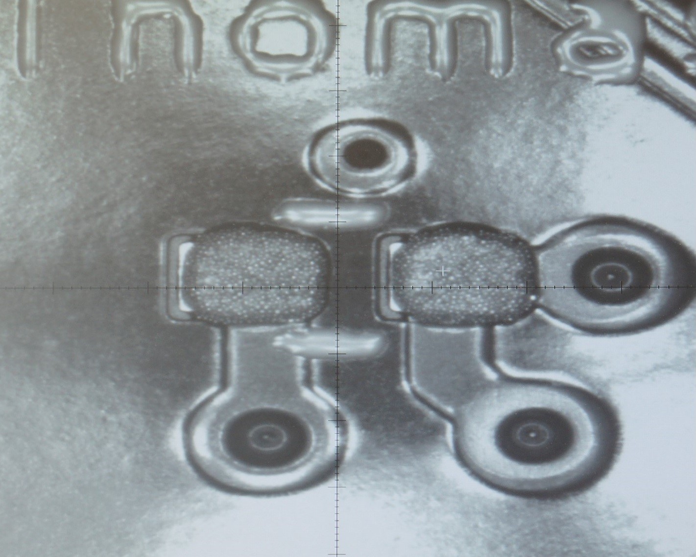
Stencil Surface Finishing
The surface quality of a stencil plays a key role in the consistency of solder paste transfer and the ease of cleaning.
We offer several finishing options depending on your production needs and budget:
🔹 Electropolishing
An advanced electrochemical process that removes microscopic peaks from the stencil surface, creating a very smooth finish.
Recommended for high-precision and fine-pitch applications where clean release of solder paste is critical.
Electropolished stencils are also easier to clean and offer excellent repeatability.
🔹 Sanding
A mechanical polishing process using fine sandpaper.
This is a standard and economical solution suitable for general applications.
It reduces surface roughness and helps remove burrs from apertures.
🔹 Etching (Deburring)
A cost-effective method to smoothen the stencil surface by light chemical etching.
Ideal for prototypes or low-volume runs.
Some light surface scratches may remain, and a small amount of solder paste may stick to the surface after printing.
Stencil Frame Options
Choosing the right stencil type depends on whether your PCB design is final and how often you plan to repeat the assembly.
🔹 Framed Stencils (with aluminum frame)
These stencils are permanently mounted on a rigid aluminum frame, which ensures excellent stability and compatibility with automatic stencil printers.
Recommended for repeatable, high-volume production where the same design is used over and over.
Although more expensive, they offer superior precision and long-term durability.
🔹 Frameless Stencils
Delivered without a fixed frame — suitable for manual printing or use with universal adjustable frames.
Ideal for prototypes, small batches, or when your PCB design may change.
More affordable and flexible, but less durable for long-term or automated use.
If you are still iterating your design, we recommend starting with a frameless stencil to keep production costs low.
Once your layout is final and production stabilizes, a framed stencil is a more reliable long-term solution.
Stencil Options for Double-Sided PCBs
For PCBs requiring SMD assembly on both sides, there are two options when it comes to stencil design:
🔹 Two Separate Stencils (Top & Bottom)
This is the recommended approach for **larger boards** and **volume production**, where separate framed stencils ensure maximum accuracy and efficiency during automated printing.
Each side of the board is processed using a dedicated stencil, ensuring consistent paste transfer and better alignment.
🔹 Combined Design on One Stencil
For **smaller boards** or **prototypes**, both the top and bottom stencil layouts can be placed side by side on a single frameless stencil.
This approach significantly reduces cost and is suitable when manual or semi-automatic printing is used.
If you're working on early-stage designs or small batch production, combining both sides into one stencil is a cost-effective and flexible solution.
For high-volume manufacturing, we recommend using two separate framed stencils for optimal performance.
Recommended Stencil Thicknesses
| Thickness | Recommended For | Description |
|---|---|---|
| 100 μm | Fine-pitch SMD components (e.g., 0603, 0402) | Most commonly used thickness. Ideal for precision solder paste application. Minimizes risk of bridging. Suitable for small components and densely populated PCBs. |
| 120 μm | Mixed component sizes | Balanced choice for assemblies combining small and mid-size components. Provides sufficient solder volume for standard SMT pads. Great for most production boards. |
| 150 μm | Large pads, connectors, or THT with paste | Best for high paste volume requirements. Suitable for large pads, power devices, or pin-in-paste applications. Not recommended for fine-pitch SMD due to risk of bridging. |
Pricing
Small
15€ *
- Size: 100×120 mm
- Thickness: 100 μm
- Material: Nickel Silver
- Lead Time: 3 WD
- Process: Chemically Etched
Medium
25€ *
- Size: 150×200 mm
- Thickness: 100 μm
- Material: Nickel Silver
- Lead Time: 3 WD
- Process: Chemically Etched
Big
30€ *
- Size: 200×200 mm
- Thickness: 120 μm
- Material: Nickel Silver
- Lead Time: 3 WD
- Process: Chemically Etched
Bigger
45€ *
- Size: 400×400 mm
- Thickness: 120 μm
- Material: Nickel Silver
- Lead Time: 3 WD
- Process: Chemically Etched