Data / Files
1. Data Provision
To ensure a fast and error-free production process, we require detailed manufacturing data along with your PCB layout.
These data files form the foundation for efficient project setup and accurate assembly.
In addition to standard Gerber and drill files, we can also process project data directly from common CAD design tools such as:
Eagle (*.sch / *.brd), Protel (*.ddb), Altium Designer (*.pcbdoc), Target3001 (*.T3001), or ODB++.
Our system supports most industry-standard formats for seamlessly data transfer.
If you do not have complete board data, please provide at least the following:
- Assembly drawing or plan (PDF or derived from Gerber data)
- Bill of Materials (BOM)
- Pick & Place file (component coordinates)
- Gerber data for stencil production (if applicable)
2. Bill of Materials (BOM)
A complete and clearly structured BOM accelerates both quotation and production stages.
The more detailed the component descriptions, the lower the risk of technical errors and clarification delays.
Your BOM should preferably be in Excel format (.xlsx) or another easily convertible file type and include the following essential information:
- Position number
- Reference designator (e.g. R1, C1, D1, IC1, etc.)
- Component type and value
- Package (e.g. 0603, 1206, SOT-223, etc.)
- Is assembled (Yes/No)
- Quantity per item
- Provided by customer (Yes/No)
- Assembly notes or remarks
- Distributor and part number
| Pos. | Part | Description | Value | Place | Manufacturer | PartName | Quantity | Provided by | Link |
|---|---|---|---|---|---|---|---|---|---|
| 1. | C1, C2 | POLARIZED CAPACITOR | 470uF | No, Yes | - | CPOL-EUE5-8.5 | 1 | ProfiAnts | www. .. |
| 2. | D1, D2 | Z DIODE | BZV55C10SMD | Yes, Yes | - | BZV55C10 SMD | 2 | ProfiAnts | www. .. |
| 3. | Q1, Q2, Q3 | PNP SOT223 transistor 1,0A,60V | BZV55C10SMD | Yes, Yes, No | - | BCP55-16 SMD | 2 | by customer | www. .. |
| 4. | R1, R2, R3, R4 | Resistor 47k | BZV55C10SMD | Yes, Yes, No, Yes | - | R-EU_M0805 | 3 | ProfiAnts | www. .. |
| 5. | X1, X2, X3 | PHOENIX miniature 2,54 | - | Yes, Yes, No | PHOENIX CONTACT | MPT 0,5/ 2-2,54 | 2 | ProfiAnts | www. .. |
| Number of components to be assembled: | 10 | ||||||||
Please remove non-electrical items (screws, washers, spacers, labels, test points, etc.) if they are not to be assembled.
3. Pick & Place File
The Pick & Place file contains the X/Y coordinates and rotation of each component and is essential for automated assembly.
It must correspond precisely with the BOM and layout.
- Reference designator / component name
- Package type
- Electrical value
- X and Y position relative to layout origin
- Rotation angle (°)
- Assembly side (TOP/BOTTOM)
Example Pick & Place File:
| Pos. | Part | Description | Value | Place | Side | X,mm | Y,mm | Rotate, ⁰ |
|---|---|---|---|---|---|---|---|---|
| 1. | C1 | POLARIZED CAPACITOR | 470uF | No | TOP | 20,32 | 7,62 | 270 |
| 2. | C2 | POLARIZED CAPACITOR | 470uF | Yes | TOP | 36,83 | 7,62 | 270 |
| 3. | D1 | Z DIODE | BZV55C10SMD | Yes | TOP | 12,7 | 8,89 | 270 |
| 4. | D2 | Z DIODE | BZV55C10SMD | Yes | TOP | 12,7 | 19,05 | 90 |
| 5. | Q1 | PNP SOT223 transistor 1,0A,60V | Yes | TOP | 19,05 | 22,86 | 0 | |
| 6. | Q2 | PNP SOT223 transistor 1,0A,60V | Yes | TOP | 25,4 | 17,78 | 0 | |
| 7. | Q3 | PNP SOT223 transistor 1,0A,60V | No | TOP | 39,37 | 22,86 | 0 | |
| 8. | R1 | Resistor | 47k | Yes | TOP | 39,37 | 15,24 | 0 |
| 9. | R2 | Resistor | 47k | Yes | TOP | 33,02 | 22,86 | 270 |
| 10. | R3 | Resistor | 47k | No | TOP | 33,02 | 15,24 | 270 |
| 11. | R4 | Resistor | 47k | Yes | TOP | 19,05 | 17,78 | 270 |
| 12. | X1 | PHOENIX miniature 2,54 | Yes | TOP | 6,35 | 13,97 | 90 | |
| 13. | X2 | PHOENIX miniature 2,54 | Yes | TOP | 48,26 | 10,16 | 270 | |
| 14. | X3 | PHOENIX miniature 2,54 | No | TOP | 49,26 | 21,59 | 270 |
4. Assembly Plan
The assembly plan should provide a clear visual reference for component placement and polarity.
It serves as a final check before production and should include:
- Component name and value
- Polarity and orientation marks
- Assembly drawing (preferably in PDF)
- Marked layout zero point in the silkscreen
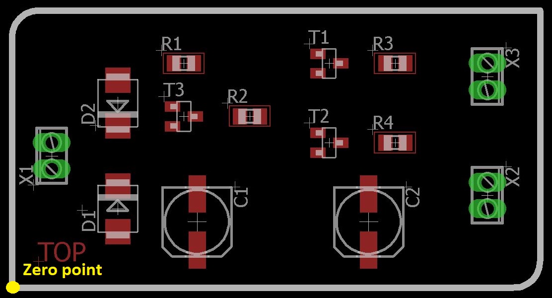
Pay attention: Missing polarity information or unclear rotation details (especially for connectors or sockets) often cause delays and assembly errors.
5. Solder Paste Stencil
We can generate solder stencil data directly from your CAD files or use supplied Gerber layers.
Please mark any pads that should not receive solder paste.
Accurate stencil data ensures consistent paste volume and reliable solder joints during SMD reflow.