Copper Plating of Conductive Traces
Copper plating of conductive traces refers to the copper layer applied to printed circuit boards (PCBs).
This layer is crucial for creating reliable electrical connections between components on the board.
Process Overview
The copper plating process includes several sequential steps that ensure proper adhesion, uniformity, and conductivity of the copper layer:
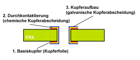
- Substrate Preparation: The board is cleaned and pre-treated to ensure strong copper adhesion.
- Through-Hole Plating: Copper is deposited inside the drilled holes to establish electrical connections between layers.
- Etching Preparation: Non-conductive areas are covered with resist, leaving only areas intended for copper coating.
- Copper Deposition: Copper is added electrolytically or galvanically to achieve the desired thickness.
- Etching Excess Copper: After achieving the required thickness, resist is removed and excess copper is etched away to form the final trace pattern.
Copper Layer Thickness
The actual distribution of the copper layer depends heavily on the PCB design — trace width, spacing, and density.
We offer three base copper thickness options: 18 µm, 35 µm, and 70 µm.
Since the base copper layer of the laminate is often insufficient for final current capacity, additional copper is applied during manufacturing.
The final copper thickness can range from 35 µm to over 105 µm depending on the design requirements.
| Base Copper | Plating Build-Up (Chem. + Galv.) | Total Copper on Surface |
|---|---|---|
| 18 µm | 25 – 42 µm | 43 – 60 µm |
| 35 µm | 25 – 42 µm | 60 – 77 µm |
| 70 µm | 25 – 42 µm | 95 – 112 µm |
Copper structures always have a height, width, and spacing between other conductive elements.
The height of a trace is determined by the base copper and the additional deposited copper layer.
Copper Thickness and Measurement Units
Copper thickness is typically measured in ounces per square foot (oz/ft²) or micrometers (µm).
Typical values range from 0.5 oz/ft² (≈17 µm) up to 3 oz/ft² (≈102 µm), depending on circuit requirements.
Importance for Electrical Performance
- Current Carrying Capacity: Thicker copper supports higher current loads, essential for power circuits.
- Thermal Management: Copper’s high thermal conductivity helps dissipate heat from components, improving reliability.
- Signal Integrity: Uniform copper layers maintain stable impedance and reduce signal loss or interference.
Minimum Trace Widths by Copper Thickness
The minimum trace width depends on the base and final copper thickness, as well as whether the PCB is plated-through (PTH) or non-plated (NPTH).
| Base Copper | Final Copper Thickness | PCB Type | Minimum Trace Width |
|---|---|---|---|
| 18 µm (Standard PTH) | 48 µm | Plated-through | 150 µm (≈6 mil) |
| 35 µm | 65 µm | Plated-through | 150 µm (≈6 mil) |
| 35 µm (Standard NPTH) | 35 µm | Non-plated | 150 µm (≈8 mil) |
| 70 µm | 100 µm | Plated-through | 150 µm (≈10 mil) |
| 70 µm | 70 µm | Non-plated | 150 µm (≈10 mil) |
All copper traces and copper areas must maintain a minimum distance of 0.5 mm from the outer board contour.
Through precise copper plating and controlled layer thickness, ProfiAnts ensures optimal electrical performance, durability, and manufacturing reliability for every printed circuit board.