Panelization, Milling, and V-Scoring
1. Panelization Guidelines
We offer full support when it comes to designing your PCB panels (panelization). Boards can be manufactured either individually or as part of a panel. This can save costs and improve handling during assembly.
The panel size can vary between 80 x 120 mm and 400 x 600 mm. If you are unable to create the panel yourself, we will be happy to assist. Normally, only identical boards are combined into a production panel. Combining different designs is possible for an additional charge.
Important Notes
- Add a perimeter margin of 5–10 mm if panels are assembled automatically
- Include fiducial marks and tooling holes
- Damaged boards are not removed but marked
Types of Panels
- Mono-panel: Same boards in a panel
- Multi-panel: Different boards in a panel
Mechanical Processing
To reduce mechanical stress during depanelization, boards can include scoring lines and/or milling bridges.
Panel with V-Scoring
- Copper to outline: 0.5 mm
- Spacing between boards: 0.00 mm
- Outline line width: 0.1 mm
- Recommended margin: 5–10 mm
- Min. PCB thickness: 0.8 mm
Panel with Milling Bridges
- Copper to outline: 0.5 mm
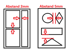
- Spacing between boards: 2.0 mm
- Outline line width: 2.0 mm
- Recommended margin: 5–10 mm
- Min. PCB thickness: unrestricted
Combination of Milling and Scoring
- Copper to outline: 0.5 mm
- Spacing (milling): 2.0 mm
- Spacing (scoring): 0.1 mm
- Outline line width: 0.1 mm
- Min. PCB thickness: 0.8 mm
Fully Routed (Milled Out) Panel
- Copper to outline: 1.0 mm
- Spacing between boards: 0.5 mm
- Outline line width: 0.1 mm
- No margin required
- Min. PCB thickness: unrestricted
2. Milling (Fräsen)
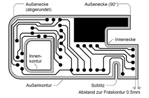
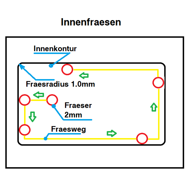
The milling outline should be drawn as a closed thin line (10 mil / 0.254 mm) on its own layer. The center of the line is used for milling regardless of the line’s width.
Internal Milling
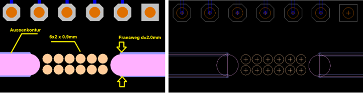
The minimum internal milling tool size is 1.0 mm, resulting in a minimum corner radius of 0.5 mm. Slots and cutouts must be included in the outline or separate drawings. For plated PCBs, internal copper cutouts will be plated by default.
General Rules
- Tool sizes of 2.0 mm and 2.4 mm are included in the base price
- Minimum tool diameter: 0.8 mm
- Minimum corner radius: 0.4 mm
- Minimum distance between copper and milling: 0.5 mm
- Avoid milling into copper – it reduces PCB durability
- Outline should be drawn with 10 mil (0.254 mm) line width
Special Milling for Rectangular Components
For precise fitting of rectangular components (e.g., 7-segment displays), additional corner drilling is recommended.
3. V-Scoring (Ritzen)
V-scoring cuts grooves on both sides of the PCB using a disc cutter at a 30° angle, leaving a residual web. This allows boards to be mounted without spacing and later broken apart.
It is widely used in automated SMT assembly processes and is suitable for PCB thicknesses of 1.0–1.5 mm.
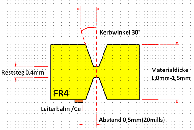
Technical Details
- Residual web thickness: 0.3–0.4 mm
- Scoring angle: 30°
- Minimum copper to scoring line: 0.5 mm
- PCB thickness: 1.0–1.5 mm
- PCB spacing in layout: 0.0 mm
Scoring Rules
- Only straight, horizontal, or vertical lines are allowed
- Lines must run from edge to edge
- Use only for rectangular boards
- Recommended only for boards ≥1.0 mm for stability