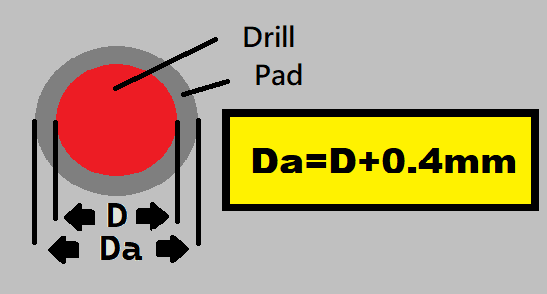
Drill annular rings and vias
All drill diameters from 0.2 mm can be produced in 0.1 mm increments. All holes are drilled 0.1 mm larger than indicated in the tool list to accommodate hole tolerances (especially after metallization). If this enlargement has already been accounted for during layout creation, it must be noted in the order. All holes (plated and non-plated) should be included in a single drill file. Non-plated holes (NPTH) must be marked. Holes with a final diameter of 6.00 mm or more are milled.
To ensure a continuous annular ring around the holes, the following minimum parameters must be maintained in the layout:
The specified values are minimums, and larger annular rings should be aimed for to enhance the functionality and reliability of the PCB.
A larger ring results in a more secure solder joint.
To ensure a continuous annular ring around non-plated holes, the following minimum parameters must also be met in the layout.
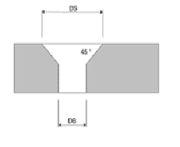
Upon request, we also apply countersinks to your PCBs. The following information is required for countersinking:
- Diameter of the hole (DB)
- Diameter of the countersink (DS)
- Side of the countersink (top or bottom layer)
Cutouts and slots are milled. If pads are present on both sides of the slots, the slots are plated through. If they are not to be plated, please provide instructions in the CAM data (Milling layer / milling file). Plated slots are producible starting from 0.8 mm (professional) and 1.0 mm (hobbyist) width.
Important: All relevant instructions must be included in the CAM data!
Edge metallization means that parts of the contour or cutouts are plated through. Contours to be metallized are milled before plating. Edge metallization is performed during the "plating" manufacturing step. After copper deposition, the edge is finished with a nickel-gold coating. Sections of the PCB contour or areas within the PCB can be partially metallized. However, since the PCB must remain in the production frame during manufacturing, the entire contour cannot be metallized. Holding bridges must be placed at certain points.
Applications of Side Plating:- Improving EMC (electromagnetic compatibility) performance
- Cooling functionality, with the edge acting as an additional heat dissipation area
- Housing connections, stable connectors, and cable connections
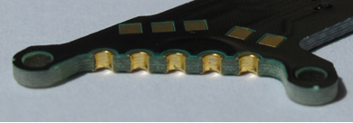
Castellated edge contacts or plated holes at the PCB edge are used as board-to-board connections, especially where PCBs with different technologies must be connected. Complex microcontroller modules, sensors, and displays are mounted and soldered onto the pads of a base PCB using SMD technology.
-
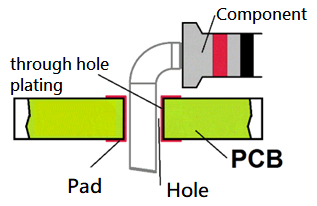
Through-Hole (Plated-Through Hole, PTH)
These are holes that extend through the entire PCB thickness. They are used for component mounting, connecting different PCB layers, and similar purposes. These holes are typically filled with metal (e.g., leaded solder) to provide electrical connectivity.
Most software automatically sets the drill and pad sizes, but what are the best values for vias? The following table provides an overview of available options:
Vias: Pad to drill Drill size Pad size mm mils mm mils 0.2 mm 8 mils 0.45 mm 18 mils 0.3 mm 12 mils 0.60 mm 24 mils 0.4 mm 16 mils 0.80 mm 32 mils 0.5 mm 20 mils 0.90 mm 36 mils 0.6 mm 24 mils 1.10 mm 44 mils -
Blind Via
A Blind Via is a type of via that connects an external layer of the PCB to one or more internal layers without passing through the entire board. It is called "blind" because it is not visible from the opposite side of the board.
Key Features of Blind Vias:Used in High-Density Interconnects (HDI): Common in HDI PCBs where minimizing space and maintaining signal integrity are critical.Space-Saving: Ideal for complex designs with high component density and fine-pitch layouts.Improved Signal Integrity: Reduces parasitic capacitance and inductance, enhancing performance for high-speed and high-frequency signals.Advantages:Efficient Use of Space: Allows routing on multiple layers while preserving space on the surface for components.Enhanced Performance: Improves electrical performance by reducing unnecessary signal paths.Compact Designs: Facilitates the creation of smaller and more lightweight devices.Disadvantages:Increased Cost: Manufacturing blind vias is more complex and expensive compared to through-hole vias.Challenging Fabrication: Requires precise control during drilling and plating processes. -
Buried Via
Buried vias are completely encapsulated within the PCB substrate, making them invisible from the surface. These vias are entirely internal to the PCB and do not appear on the outer layers. They are used to create connections between internal layers.
Key Features of Buried Vias:Layer Connection: Buried vias only connect internal layers of a PCB. For example, in an 8-layer PCB, a buried via might connect layer 3 to layer 6, bypassing the outer layers (1, 2, 7, and 8). Invisible on Surface: Since they are contained within the PCB, they do not occupy surface space, leaving more room for surface components and routing. Compact Design: Buried vias enable complex, high-density designs by allowing connections between layers without disrupting surface routing.
Advantages:Space-Saving: They free up surface space, enabling denser component placement and more efficient routing.Enhanced Signal Integrity: By keeping critical signal paths internal, they can reduce electromagnetic interference (EMI) and improve performance.Improved Heat Management: Internal vias can help distribute heat within the PCB more effectively.Aesthetic: Since buried vias are not visible on the outer layers, the PCB can have a cleaner appearance.Disadvantages:Cost: Manufacturing PCBs with buried vias is more expensive due to the additional drilling and lamination processes required.Complexity in Manufacturing: The fabrication process involves advanced techniques like sequential lamination, which can increase production time and complexity.Inspection Challenges: Since buried vias are internal, it’s harder to inspect and detect defects compared to through-hole vias. -
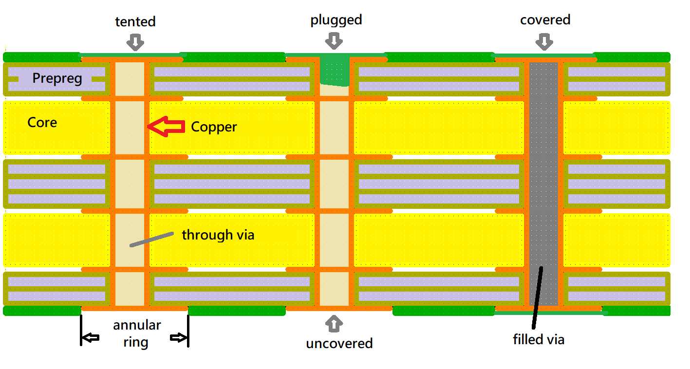
Tented Vias
"Tented" refers to holes in the PCB that are covered with solder mask during the screen printing process. This process seals the holes by covering them with solder mask to prevent liquids or contaminants from entering. The goal is to isolate the via from the external environment, either fully or partially. Sealed holes are being protect from corrosion.
-
Plugged
"Plugged" refers to holes that are filled with material such as resin or paste to prevent liquids or contaminants from entering. These holes can be drilled or opened, but are then filled with material to seal them and protect them from moisture or other harmful influences.
-
Filled
"Filled" refers to the process of filling holes in the PCB with special material such as epoxy resin. This process is used to reinforce the PCB and increase its mechanical strength. Filled holes can be useful for applications that require a more stable and robust circuit board.
-
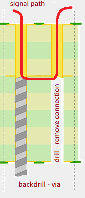
Back drilling
This is a process used in multilayer PCBs to remove unused portions of plated through-hole (PTH) vias that can cause signal integrity issues, especially in high-speed and high-frequency circuits.
Why is Back Drilling Needed?
Signal Integrity:In high-speed PCB designs, via stubs (unused portions of vias that extend beyond the layer where they are connected) can create reflections and distortions in the signal.
Impedance Control:Via stubs add unwanted capacitance and inductance, which affect the controlled impedance of the PCB traces.
Minimize Crosstalk:Stubs can act as antennas, picking up or radiating electromagnetic interference (EMI), leading to crosstalk between signals.
Reliability:Back drilling removes unnecessary material, reducing stress on the via and improving reliability.
Key Considerations for Back Drilling Design Specifications:Back drilling must be planned during the PCB design phase. Designers specify the layers to which the via connects and where back drilling should stop.
Drill Depth:The depth of the back drill is critical and needs precise control to avoid damaging the connected layers.
Stack-Up Design:Proper stack-up planning minimizes the need for excessive back drilling.
Fabrication Costs:Back drilling adds complexity and cost to the manufacturing process. It’s generally used only where necessary for signal integrity.
Alternatives to Back Drilling Blind/Buried Vias:These vias only connect specific layers and do not extend through the entire PCB.
Microvias:Smaller vias used in HDI (High-Density Interconnect) designs, which reduce or eliminate stubs.
Controlled Impedance Design:Optimizing via structures to minimize stub effects without additional drilling.