Solder Mask: Functions and Design Guidelines
1. Functions and Characteristics of the Solder Mask
The solder mask (also known as solder resist or solder stop) serves the following purposes:
- Protection against short circuits during soldering
- Insulation of the PCB surface from other elements (e.g., components or enclosures)
- Protection of the PCB against mechanical or chemical influences
- Improved electrical properties through better insulation values
In our production, we use a two-component photosensitive solder resist. The lacquer is applied using the screen printing process and is then processed using photolithography.
The thickness of the solder mask is approximately:
- ~27 µm over the copper traces
- ~36 µm over the base material
2. Design Guidelines
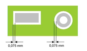
Clearance:
The clearance (oversize) between the solder mask and the pads should ideally be 0.2 mm (0.1 mm around each side). This clearance is either included by the customer in the dataset or added by us during production.
3. NDK Holes (Non-Plated Through Holes):
Non-plated through holes (NPTH) must be excluded from the solder mask to prevent lacquer residue in the holes. The clearance should be 0.4 mm in total (0.2 mm around).
4. Metallized Contours:
Metallized contours, cutouts, and slots must also be excluded from the solder mask, similar to NPTH holes.
5. Connector Fingers:
Connector fingers must be completely free of solder mask. It is not advisable to leave solder mask bridges between the contact pads.