Marking Print (Component Identification)
1. Purpose and Properties
The marking print (also known as silkscreen or position print) serves the following purposes:
- Identification of component positions
- Service markings
We use a two-component paint for the marking print, applied using the screen printing process.
2. Design Guidelines
Clearance:
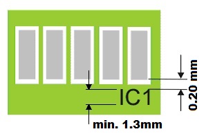
Solder pads must not be covered by the marking print. This can cause issues during soldering, assembly, and electrical testing. A minimum clearance of 0.2 mm must be maintained between contact surfaces and marking print.
- Text and lines overlap pads
- Difficult to read
- Pads not accessible for E-test
- Problems during SMD soldering
- Clear and easy-to-read marking
- Pads remain accessible for testing
- No issues during soldering
If we detect any solder pad that is covered (clearance < 200µm), we will remove the marking print in that area during processing.
Text and Line Dimensions
- Minimum line width: 0.254 mm
- Minimum text height: 1.3 mm
To ensure legibility, both text height and line thickness must not be too small. The recommended ratio of text height to line width is between 15:1 and 8:1. The ideal ratio is 60 mil height / 8 mil line width.