Layer Orientation
Separate data files must be created for each layer (TOP and BOTTOM).
Each layer must be clearly labeled.
💡 It is recommended to include identifying text (either inside or outside the board area) on each layer.
Please always label your circuit boards with TOP and BOT directly in the copper layers.
⚠️ Important:
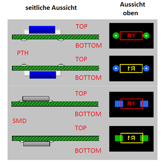
Top layer – text should always be readable.
Bottom layer – text must be mirrored.
Please do not make the text too small!
Texts are etched along with the copper traces and must follow the same design rules.
Texts are etched along with the copper traces and must follow the same design rules.
The minimum line width should not be less than 0.254 mm, and the text height should not be smaller than 1.3 mm.
🧮 Two-Layer Boards
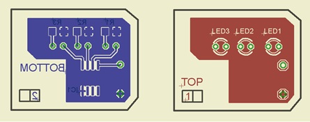
The word “TOP” should be readable, while the label “BOT” on the bottom layer should be mirrored.
Please note: the mirrored BOT text will appear correctly once the circuit board is fully assembled.
🧩 Multilayer Boards
Always label your multilayer boards with TOP and BOT in the copper layers.
Inner layers should also be labeled — the order is very important!
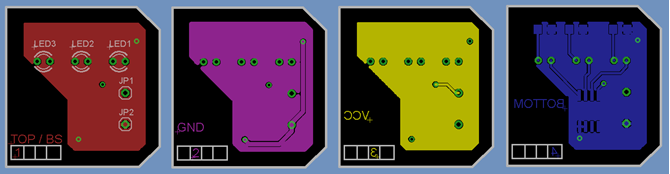
🔢 The layer sequence can be indicated in different ways:
One common method is to enter layer numbers directly in the copper image, using logical numbering for each layer:
- 1 for the top layer
- 2 for the next inner layer, then 3, and so on
- The final number represents the bottom layer
🗂️ File Naming Convention for Each Layer
When providing your design files in Gerber format, it is a good practice to use standardized file extensions that clearly indicate which layer each file corresponds to.
The following table outlines the recommended naming convention for layer exports.
Including TOP and BOTTOM labels directly on the PCB, together with consistent file naming, helps minimize the risk of manufacturing errors.
| File Name | Corresponding Layer |
|---|---|
| pcbname.GTL | Top copper layer |
| pcbname.GBL | Bottom copper layer |
| pcbname.GTS | Top solder mask |
| pcbname.GBS | Bottom solder mask |
| pcbname.GTO | Top silkscreen (legend) |
| pcbname.GBO | Bottom silkscreen (legend) |
| pcbname.GKO / boardname.GM1 | Board outline (mechanical layer) |
| pcbname.G2L | Inner layer 2 (for four-layer boards only) |
| pcbname.G3L | Inner layer 3 (for four-layer boards only) |
| pcbname.XLN | Drill file (drill map / drawing) |
Ensure that the positions, attributes, and quantities of all holes are correctly defined.
Providing the drill layer (.XLN) is strongly recommended to avoid alignment or tooling issues.